
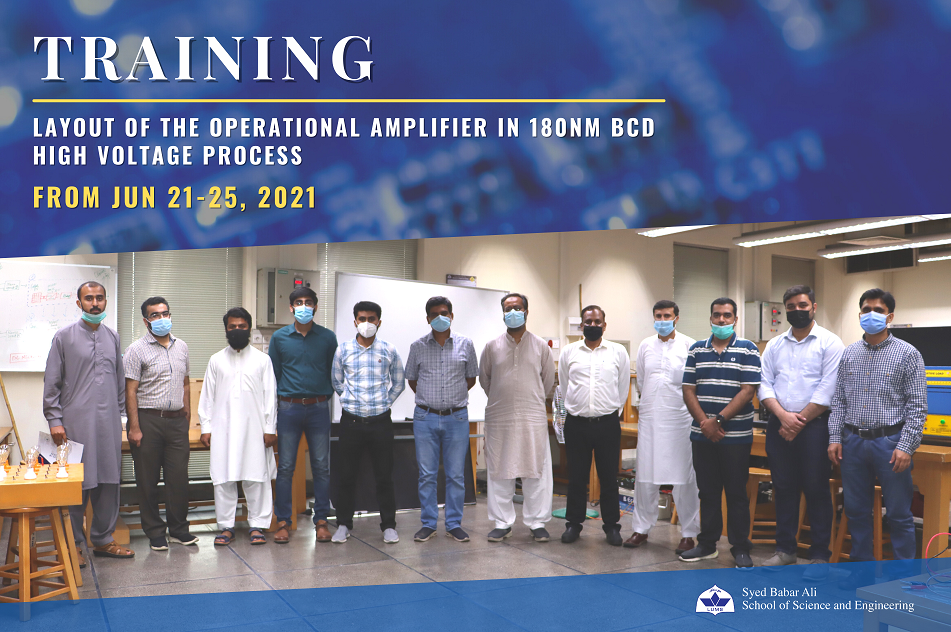
Training: Layout of the Operational Amplifier in 180nm BCD High Voltage Process
Specific training of Integrated Circuit (IC) Design focused on Layout of the operational amplifier in 180nm Bipolar CMOS & Deep-Trench (BCD) High Voltage Process was held at Electrical Engineering Department (EED), Syed Babar Ali School of Science and Engineering (SBASSE), LUMS. The training was planned for the scientists and engineers of the National Electronics Complex of Pakistan (NECOP). The training was conducted by Dr. Awais Bin Altaf, Assistant Professor, EED, SBASSE, LUMS and was attended by 10 (ten) NECOP participants. The five days, eight hours per day, training focused on the layout design, design rule check (DRC), layout vs schematic (LVS), post-layout simulation, and final sign-off process for the chip fabrication (taepout). The trainees performed all these tasks in the Embedded Lab in EED using industry-standard Cadence and Mentor Graphics CAD tools for the IC design. This training will help in bridging the gap between industry and academia, and will lead to future joint collaborative efforts in the area of IC design.
This training took place between June 21st and 25th, 2021.
The NECOP participants also engaged during their visit with the EED external relation committee (ERC) and discussed mutual projects of interest. The training concluded with a closing ceremony chaired by Dr. Abubakr Muhammad (Head of Department, EED) and Dr. Sabieh Anwar (Dean, SBASSE).