Event date:
May
20
2021
11:30 am
Modulating the Optical Properties of 2D Molybdenum Disulfide by Applying the Strain through Nematic Liquid Crystal
Supervisor
Dr. Ammar Ahmed Khan
Dr. Ata Ulhaq
Student
Muhammad Kashif Boota
Venue
Zoom Meetings (Online)
Event
MS Thesis defense
Abstract
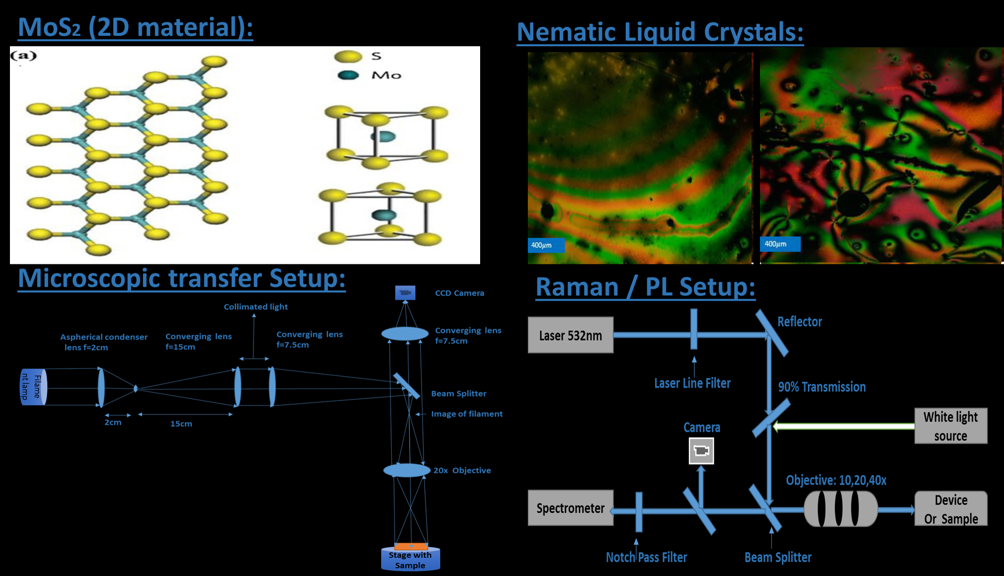
The principal aim of my senior project is to investigate the characteristics (optical and electrical) of extremely thin two-dimensional material such as Molybdenum Disulfide (MOS_2) for various kinds of substrates such as Si, glass, and ITO coated glass substrates. Two-dimensional (2D) materials are becoming increasingly popular due to their electrical and optical properties that can be used in the manufacturing of 2-D devices such as single-photon emitters. Desired MOS_2 flakes were exfoliated and transported to a specific position on substrates (Silicon, glass, ITO coated glass). The electrical and optical properties of the transferred flake were supervised via electrical measurements, Raman Spectroscopy, and Photoluminescence spectroscopy. The optical characterizations accomplished using Raman and Photoluminescence spectroscopy allowed us to ascertain the atomic thickness of the transferred flake. The conclusion of Raman and Photoluminescence Spectroscopy revealed successful deposition of an extremely thin layer of MOS_2 flake. In addition, studies regarding the effect of electric field variation on a thin MOS_2 flake transferred on an ITO coated glass cell manifested an increase in luminescence with an increase in the electric field.
The subsequent objective of my Thesis is to bring about studies leading to the evolution of single-photon devices by making the use of extremely thin layers (mono) of MOS_2 flake. This kind of device will be, it emits modulated pulses of photons. In order to manufacture a single photon emitter from monolayer MOS_2, physical defects must be induced in MOS_2 (in our case 5CB will do that)in order to create potential wells that can trap excitons (electron-hole pair generated after excitation of an electron from the valence to conduction band).
The subsequent objective of my Thesis is to bring about studies leading to the evolution of single-photon devices by making the use of extremely thin layers (mono) of MOS_2 flake. This kind of device will be, it emits modulated pulses of photons. In order to manufacture a single photon emitter from monolayer MOS_2, physical defects must be induced in MOS_2 (in our case 5CB will do that)in order to create potential wells that can trap excitons (electron-hole pair generated after excitation of an electron from the valence to conduction band).
Meeting Link: https://lums-edu-pk.zoom.us/j/99523973973?pwd=UnhFRmJEd1YwTzQxVXNxOWszUmJFUT09
Meeting ID: 995 2397 3973
Passcode: 680189

