
Optoelectronic Properties of van der Waals Heterostructures Formed at the Transition Metal Dichalcogenide and Organometallic Perovskite Interface
Abstract:
The main focus of this research is to make a hybrid coupled heterojunction system. Two-dimensional (2D) perovskites had been tested to demonstrate suitability for optoelectronic devices due to bandgap tunability and higher stability in ambient conditions as compared to their 3-dimensional (3-D) counterparts. At the same time, which twodimensional transition metal dichalcogenides (TMDCs) demonstrate exceptional optical and electronic properties, the atomically thin layer thickness intrinsically limits often overall light absorption and optoelectronic device performance. It has been demonstrated in recent work that the strong coulomb interaction gives rise to interlayer excitons, where electrons and holes are spatially separated in different bands revealing their ultrafast formation, long lifetimes, and intriguing spin-valley dynamics.
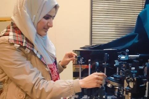
In our work, we aim to design heterojunction of monolayer MoS2/(BA)2PbI4 perovskite to achieve robust interlayer coupling, more efficient charge and energy transfer. MoS2 flakes and perovskite thin films are fabricated using mechanical exfoliation method that are stamped together by transfer setup to form electrically coupled heterojunction system. To investigate optoelectronic properties of this heterojunction system, Raman spectroscopy and Photoluminescence spectroscopy were performed. In addition to making heterostructures with lead halide perovskites, which aren’t very desirable due to the toxicity of lead, we also discuss ongoing work on Bismuth(Bi)-based perovskite heterostructures to replace lead and broaden lead free perovskite films.
![]()
Connect
![]()
![]()
![]()
![]()
![]()